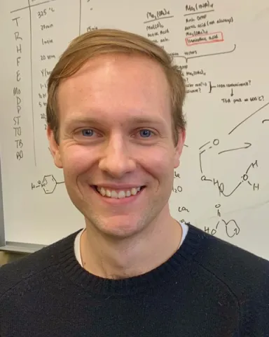
Scholar Spotlight: Reynolds L. Dziobek-Garrett
Reynolds L. Dziobek-Garrett – JCM Foundation Scholar
1st Year Scholar, PhD Candidate, Chemistry
Johns Hopkins University
Research:
Research focuses on controlling the properties of atomically-thin semiconductors via chemical synthesis. He uses high-resolution electron microscopy and laser spectroscopies to understand the role of crystalline defects formed during growth of these “2D” materials, which have applications in nanoscale electronic and quantum devices.
Describe the expected benefit of your research to society:
The rapidly growing global demand for computing capability drives Moore’s Law, which predicts a doubling of computing power every two years through the development of ever-smaller transistors. This demand stands at odds with current sustainability trends, however, as state-of-the-art silicon-based transistors use increasing amounts of energy and contribute to a significant carbon footprint for these processes.
To mitigate the climate effects of this sector, while still meeting computing demand, new semiconductor materials are required to replace current silicon-based microelectronics and therefore reduce overall power consumption. Two-dimensional semiconductors stand as the leading class of materials to reduce this power consumption in the near and long-term. These materials enable continued transistor scaling while reducing power loss and waste heat output when applied in computing processes. To be industrially relevant, however, these devices must be produced en masse. The two-dimensional semiconductor materials developed through my research will directly address this need and enable the production of new computer chips which process larger volumes of information more quickly while using less electricity and producing less waste heat. I will use inherently scalable techniques to answer key questions in material growth, driving progress towards large-scale synthesis of these materials to redefine the frontiers of chip production and application.
Career objectives:
I aim to work in the semiconductor industry, helping integrate new materials into commercial technologies. I am excited about the opportunity to address long-term problems facing the adoption of materials—such as the 2D semiconductors I currently study—which can increase the energy efficiency of future computer chips. This is known as a “lab to fab” transition, where I will use industrial methods to scale up my current research to the needs of commercial production. I also aim to use my position to establish ties with academic institutions and help students, especially of underrepresented backgrounds in the physical sciences, to understand commercial fabrication processes. Through this career development outreach, I hope to share my knowledge and empower young scientists to connect more effectively with their own research, build excitement about its impact, and share insights and knowledge that can be taken “from the fab back to the lab.”
- Log in to post comments

